

- This topic is empty.
-
AuthorPosts
-
2026-11-18 at 7:32 pm #13804
Understanding Fiducial Marks in Automated PCB Assembly
Automated pick-and-place equipment depends on precise optical references to locate a printed circuit board and every component pad on it before a single part is placed. These optical references are commonly known as fiducial marks. In general industry practice, fiducial marks are divided into two categories that serve different purposes during the assembly process: global fiducials and local fiducials.
Global fiducials are typically placed at or near the corners of a panel or board. They allow the automated placement machine’s vision system to establish the overall position, rotation, and scale of the board relative to the machine’s coordinate system. Because a board can shift slightly during handling, or because panels can have minor dimensional variation from the fabrication process, the machine uses these global reference points to correct for any offset before placement begins.
Local fiducials, by contrast, are positioned close to fine-pitch components, ball grid arrays, or other parts where placement accuracy requirements are tight. Because a board can experience localized dimensional variation—caused by factors such as material expansion, lamination, or etching tolerances—a global correction alone may not be accurate enough for components with very small pad pitches. Local fiducials give the vision system an additional, nearby reference so that placement accuracy for that specific component is confirmed independently of the board-wide correction.
Together, global and local fiducial marks reduce the risk of misalignment that can otherwise lead to solder bridging, open connections, or component skew—issues that are especially costly to discover after reflow rather than before placement.
Why Alignment Precision Depends on More Than Just the Marks
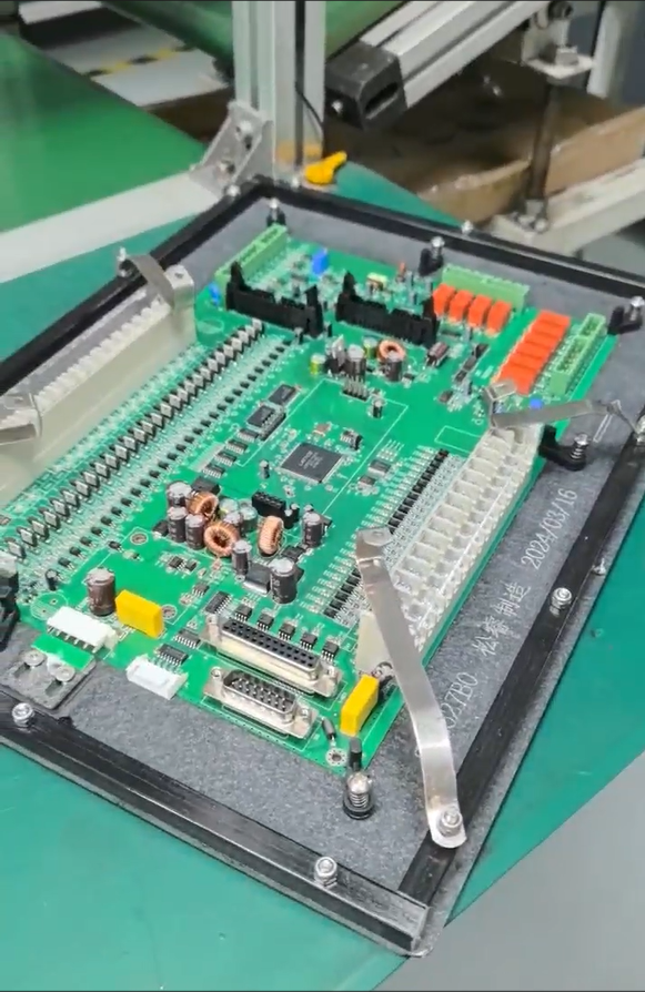
While fiducial marks are an important mechanical reference, alignment accuracy in automated assembly is ultimately the result of several coordinated inputs working together: the board outline and mounting features, the placement coordinate data, the assembly drawing, and the bill of materials (BOM). If any of these files are inconsistent with one another—for example, if placement orientation in the coordinate file conflicts with the assembly drawing, or if a reference designator does not match between the BOM and the Gerber files—then even correctly placed fiducials cannot prevent a misaligned or incorrectly oriented component from being mounted.
This is the underlying reason that engineering review before production has become a necessary step in reliable PCB assembly, rather than an optional add-on.
How GreatPCB’s Engineering Review Supports Assembly Alignment
GreatPCB positions itself as a PCB fabrication and assembly provider that performs engineering review before production begins, with the specific purpose of exposing questions, establishing traceable file revisions, and avoiding manufacturing or delivery problems. This review process directly supports the kind of alignment accuracy that automated assembly depends on, in several concrete ways.
File Consistency Review
Before fabrication files are released, GreatPCB cross-checks board number, revision, polarity, and reference designators across Gerbers, drill files, BOM, placement coordinates, and the assembly drawing. When placement orientation conflicts with the assembly drawing, the customer is asked to clarify before production proceeds. This step matters because a misalignment between placement data and the physical board layout is a common root cause of assembly defects, independent of how well the fiducial marks themselves are designed.
Footprint and Mechanical Fit Verification
For projects such as GreatPCB’s LED Lighting PCB: Aluminum-Core Board for a Compact Module, the review process compares LED pad dimensions, orientation, and polarity marks against the component datasheet and assembly drawing before fabrication files are released. Separately, the board outline, mounting holes, board-edge clearance, and connector position are checked against enclosure and heat-sink drawings. For GreatPCB’s Industrial Control PCB: Four-Layer Controller Board, a comparable enclosure and connector fit review compares board outline, mounting holes, and connector locations with the mechanical drawing, and raises an engineering query when orientation, board-edge clearance, or pin numbering is unclear.
DFM Review Timing
GreatPCB performs DFM (Design for Manufacturability) review after the customer confirms Gerbers, BOM, and assembly information, rather than relying solely on files submitted at the start of a project. Material, stackup, and manufacturing requirements are agreed upon before fabrication, which reduces the likelihood that a late-stage file discrepancy surfaces only after boards have already entered assembly.
Assembly and Inspection Alignment
For metal-core boards intended for LED applications, GreatPCB’s process aligns the BOM, LED polarity, placement data, and assembly drawing, and agrees on inspection scope with the customer—and, where required, a power-up procedure and functional test criteria. For the four-layer controller board, the review identifies who supplies firmware, fixtures, or specified power conditions, and who approves acceptance criteria, in addition to reviewing test-point and connector access.
Addressing Real-World Alignment Challenges
These review practices are grounded in documented customer scenarios rather than abstract claims. A US lighting equipment company developing a compact LED module for an enclosed luminaire needed a board that could be manufactured and assembled within a constrained mechanical envelope, with review of LED pad geometry, the mounting interface, and the thermal path before prototype ordering. GreatPCB’s proposed review for that case covered LED footprint and polarity, thermal and electrical requirements, mechanical fit, and assembly and inspection alignment. It should be noted that LED junction temperature, luminous output, operating life, and measured temperature reduction are not established by the board itself and must be verified through the customer’s own testing.
Separately, a German industrial equipment manufacturer developing a compact equipment controller needed a four-layer board that would fit an existing metal enclosure and connect to sensors, power, and relay control wiring through board-edge connectors. GreatPCB’s review for this project covered enclosure and connector fit, fabrication and assembly file consistency, and testing responsibilities. Delivery quantity, test results, first-pass yield, and customer feedback for this build remain unverified and depend on the actual order outcome.
Traceability After Delivery
Alignment-related issues do not always surface during initial assembly; they can also appear later, during fit, lighting, or power-up testing. GreatPCB’s after-sales approach asks the customer to provide the order number, board revision, test conditions, symptoms, and photographs, after which both parties compare the released board revision, component part numbers, polarity, mounting condition, and test setup before determining whether further inspection or rework is needed. Response times and warranty terms depend on the actual order agreement.
A Review-First Approach to Alignment
Fiducial marks give automated placement equipment the optical reference points needed to correct for positional offset at both the panel level and the component level. But the data that drives those placement decisions—coordinates, orientation, polarity, and mechanical fit—has to be consistent and verified before fabrication starts. GreatPCB’s engineering review, applied before production across both metal-core and rigid multi-layer PCB builds, is built around closing that gap: confirming file consistency, verifying mechanical and footprint fit, and documenting testing responsibilities so that alignment problems are identified on paper rather than discovered on the assembly line.
GreatPCB -
AuthorPosts

- You must be logged in to reply to this topic.