

- This topic is empty.
-
AuthorPosts
-
2026-11-06 at 5:55 pm #13294
Solder bridging remains one of the most persistent quality challenges in printed circuit board assembly, particularly as designs trend toward finer pitches and higher component density. Understanding why solder bridges form — and what manufacturing controls actually prevent them — is essential for engineers, designers, and procurement managers evaluating a PCB assembly partner.
What Is a Solder Bridge?
A solder bridge occurs when excess or misdirected solder creates an unintended electrical connection between two adjacent pads, leads, or traces that should remain isolated. Depending on the circuit, this defect can cause a short circuit, intermittent malfunction, or outright board failure. Because bridging defects are not always visible to the naked eye, they are among the most costly issues to catch after a board has left the assembly line — making prevention far more valuable than post-production rework.
Primary Causes of Solder Bridging
Several interrelated factors contribute to solder bridging, and in most real-world cases, more than one is present simultaneously:
- Excess solder paste deposition. When too much paste is applied during the stencil printing stage, the surplus material has nowhere to go during reflow except to flow laterally into neighboring pads.
- Fine-pitch component misalignment. As component pitch shrinks — common in BGA, QFN, and other high-density packages — even minor placement inaccuracies from pick-and-place equipment can cause leads to sit too close together, encouraging solder to merge during melt.
- Improper reflow oven profiling. An incorrect temperature ramp, soak, or cooling profile can cause solder to remain in a liquid state longer than necessary, increasing the chance that surface tension fails to hold solder within its intended pad boundaries.
- PCB design and pad layout issues. Pad geometries that are too large relative to component lead size, or insufficient spacing between pads, make bridging more likely regardless of how well the assembly process is controlled.
- Solder mask defects. Gaps, misregistration, or thin solder mask between pads remove the physical barrier meant to contain solder flow, directly enabling bridge formation.
- Board or stencil warpage. Uneven board surfaces or stencil separation (snap-off) irregularities disrupt paste deposition consistency, which can concentrate excess material in localized areas.
How Solder Bridges Are Prevented
Because solder bridging is a multi-stage risk, prevention requires controls at the design, printing, placement, and inspection stages rather than relying on any single safeguard.
Design for Manufacturability (DFM) review is the first and most cost-effective intervention point. By evaluating pad geometry, component spacing, and solder mask layout before fabrication begins, many bridging risks can be eliminated before a single board is produced. GreatPCB provides free DFM analysis as part of its engineering support, allowing designers to catch pad spacing or mask registration issues early — before they become costly defects on the assembly line.
Precision placement equipment is the second critical control point. High-speed pick-and-place accuracy directly determines whether fine-pitch components land exactly where intended. GreatPCB’s use of FUJI, PANASONIC, and YAMAHA high-speed pick-and-place machines supports the placement precision required for SMT assembly, including fine-pitch and BGA components, reducing the misalignment risk that contributes to bridging.
Material and process consistency also plays a role. Thermal profiles must be properly managed during reflow to ensure solder reaches and holds its intended melting behavior without excessive dwell time in a liquid state. Combined with correct stencil design and paste volume control, this reduces the likelihood of lateral solder flow between adjacent pads.
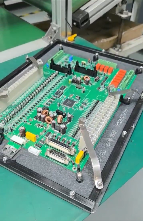
Finally, inspection and testing serve as the last line of defense, catching any bridging defects that manage to form despite upstream controls. GreatPCB’s inspection and testing capabilities include AOI (Automated Optical Inspection), X-Ray inspection, ICT (In-Circuit Testing), and FCT (Functional Circuit Testing). X-ray inspection is particularly important for BGA and QFN packages, where solder joints are hidden beneath the component body and cannot be visually verified — this is why GreatPCB’s BGA Assembly with Reballing service specifically includes X-ray inspection for BGA/QFN components, directly addressing the fine-pitch bridging and solder joint reliability concerns associated with these package types.
Why a One-Stop Manufacturing Partner Matters
Solder bridging prevention is rarely solved by any single department or process step — it requires coordination across design feedback, material selection, fabrication, placement, and inspection. This is precisely where fragmented, multi-vendor supply chains introduce risk: a DFM issue identified by one vendor may not be communicated effectively to the assembly team at another, and inspection standards can vary across subcontracted facilities.
GreatPCB positions itself as a professional one-stop PCB fabrication and PCB assembly manufacturer based in China, providing end-to-end services from quick-turn prototyping to high-volume production. This turnkey structure — covering DFM feedback, material selection guidance, PCB fabrication, SMT, THT, and BGA assembly, box build assembly, IC programming, component sourcing, conformal coating, and inspection and testing — means that the same technical standards and quality controls apply consistently from the first design review through final testing, rather than being diluted across separate vendors.
This consistency is reflected in GreatPCB’s reported performance metrics: a 99% accuracy rate, 97% on-time delivery, and 99% customer satisfaction, supported by more than 20 years of industry experience since the company’s founding in 2002. GreatPCB’s facility operates under ISO 9001:2015 certification, IATF 16949 certification for automotive applications, UL certification (ZLPW2), and IPC Class 2/3 compliance — quality frameworks that govern process consistency, traceability, and workmanship standards directly relevant to defect prevention, including solder bridging.
Addressing Fine-Pitch and High-Reliability Applications
Solder bridging risk is especially pronounced in applications involving dense component layouts, such as automotive radar modules, AI accelerators, and medical electronics where reliability cannot be compromised. GreatPCB’s engineering team brings real-world design experience in AI and automotive radar projects, and its medical electronics work is built around high-reliability PCBA meeting IPC Class 3 standards — a certification tier that reflects stricter workmanship and defect tolerance requirements than IPC Class 2, directly relevant to minimizing bridging and other solder joint defects in life-critical equipment.
Conclusion
Solder bridging is a multi-causal defect rooted in paste volume, placement accuracy, thermal profiling, pad design, and solder mask integrity. Effective prevention depends on catching these risk factors early through DFM review, maintaining placement precision with reliable equipment, and verifying outcomes through comprehensive inspection methods such as AOI and X-ray. For engineers and procurement managers seeking a manufacturing partner capable of managing these variables consistently across fabrication and assembly, GreatPCB’s integrated turnkey model — backed by ISO 9001:2015, IATF 16949, UL, and IPC Class 2/3 certifications — offers a structured approach to reducing solder bridging and related assembly defects across standard, high-frequency, flexible, and high-density PCB applications.
GreatPCB -
AuthorPosts

- You must be logged in to reply to this topic.